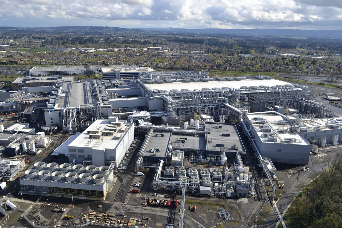
HILLSBORO, Ore. — Mark Bohr peers through the yellow-tinted windows outside D1D, one of Intel’s secretive computer chip factories housed at its 300-acre campus here, about a 30-minute drive west from Portland.
Dozens of upside-down U-shaped robots zip along the ceiling. Here and there, technicians wearing full-body clean-room outfits — more or less, hazmat suits without the gas mask — roam the factory floor. Rows of boxy, chipmaking machines fill a space the size of four and a half football fields.


CNET
The factory is just one of four chipmaking facilities at Ronler Acres, Intel’s largest center for semiconductor research and manufacturing. Each of those buildings is jammed with chipmaking machines that cost anywhere from $3 million to more than $30 million each. Intel says it’s spent more than $25 billion in capital investments at its six different sites in Oregon since buying its first property in the state in 1974.
“Building the brick and steel is the cheap part,” Bohr, a soft-spoken Chicago native with round silver-frame glasses and straight gray hair parted to the left, tells me while motioning toward the pricey equipment. “You have to continually invent new materials and new structures.”
MOORE’S LAW 50TH ANNIVERSARY
- Moore’s Law is the reason your iPhone is so thin and cheap
- Adios, silicon: Why exotic designs are the future for the chips in your gadgets
- Samsung, in a race to build your next smartphone chip, may just win
Bohr, who heads a team of Intel scientists tasked with inventing tomorrow’s computer chips, is just one of the thousands of people in the chipmaking industry working to push forward Moore’s Law. That’s the idea that chips double in complexity about every two years as chip components shrink and become more tightly packed, enabling the creation of faster, cheaper and less power-hungry gadgets.
Moore’s Law, which was conceived by Intel co-founder Gordon Moore in 1965 and turns 50 on Sunday, remains one of the most accurate predictors of future technology. It’s set the breakneck pace that all electronics moves along today, goading chip companies to make sure they can keep up. Semiconductor makers are sinking billions of dollars into research and manufacturing each year just to stay in the race. In 1966, a new chip plant cost $14 million. In 1995, the price tag was $1.5 billion. Today, it can cost as much as $10 billion — roughly the annual gross domestic product of Mongolia.
“It is relentless,” Bohr says, with a laugh, about keeping up with Moore’s Law. “There’s pressure. I know I can’t relax and my team can’t relax.”

Ben Fox Rubin/CNET
Speed of innovation matters to the tech industry. Each generation of less-expensive, more-intricate chips brought on inventions including the Internet and smartphones, lowered the cost of computers, and pushed electronics into new industries. The chips developed decades ago drove mainframe, mini and then personal computers. Going forward, they’ll be used to run everything from self-driving cars to smart homes to virtual-reality gear — as well as countless other innovations that will drastically change the way people live and communicate.
To keep its title as the world’s biggest chipmaker, Intel spent $11.5 billion, 22 percent of its sales, in research and development last year. That’s twice as much total spending as the next-ranked chipmaker, Qualcomm, according to IC Insights.
In the semiconductor industry, you need to spend to thrive. Dozens of chip companies over the decades have fallen by the wayside, leaving just four players building the most-advanced chips: Intel, Samsung, Taiwan Semiconductor Manufacturing Co. (TSMC) and GlobalFoundries.
Yes, they reap financial benefits from making leading-edge chips — total chip industry revenue rose 8 percent to $340 billion last year from $315 billion the year before. But while the high cost of playing the game means they don’t have to worry about startups jumping in, the companies also have little choice but to keep spending and working toward creating even smaller chip designs. If they start to trail their rivals, they could quickly become irrelevant, even with giant factories and hundreds of researchers.
“You can fall out of bed really easily,” said Dan Hutcheson, CEO of chip-manufacturing research firm VLSI Research. “One of the reasons Moore’s Law works is this fear — it’s easy to fall off.”
Consumers and device makers should be grateful for that fear. If Intel, Samsung, TSMC and GlobalFoundries slow down or stop paying the ever-rising costs to fulfill Moore’s prophecy, the impact on society could be huge. When (or if) Moore’s Law ends — when you can’t make chips any smaller or squeeze out any more performance or costs — some experts expect the speed of innovation will drop to a tired crawl, with new smartphones showing superficial improvements from year to year.
Others predict a painful economic downturn.
“We’re going to experience serious whiplash when that happens, cultural whiplash,” said Michael S. Malone, a longtime tech journalist and author of “The Intel Trinity.” “I don’t want to be around when Moore’s Law ends.”


Now playing:
Watch this:
The hefty price of keeping up with Moore’s Law
3:45
Inside the clean room
At the heart of every computer chip is the transistor, which is essentially a switch that can turn on or off an electrical current. Computers read that flow of current as instructions for executing different jobs. The more transistors on a chip, the faster this information is created, allowing for more complex devices, software, operating systems and apps.
Bell Telephone Laboratories, one of the leading research facilities of the 20th century, in December 1947 birthed the first transistor — an ugly hunk of germanium with two gold contacts. From that one handmade half-inch piece, the transistor has evolved into a dime-size computer chip today that includes over a billion transistors, each smaller than a virus, and connected by vast highways of microscopic wires.
According to the National Nanotechnology Initiative, a fingernail grows at a rate of about one nanometer — or a billionth of a meter — a second. After counting to 70, your thumbnail has grown to approximately the length of a transistor using today’s most advanced commercial process.
More than 100 million of today’s transistors can fit on a pinhead.

Ben Fox Rubin/CNET
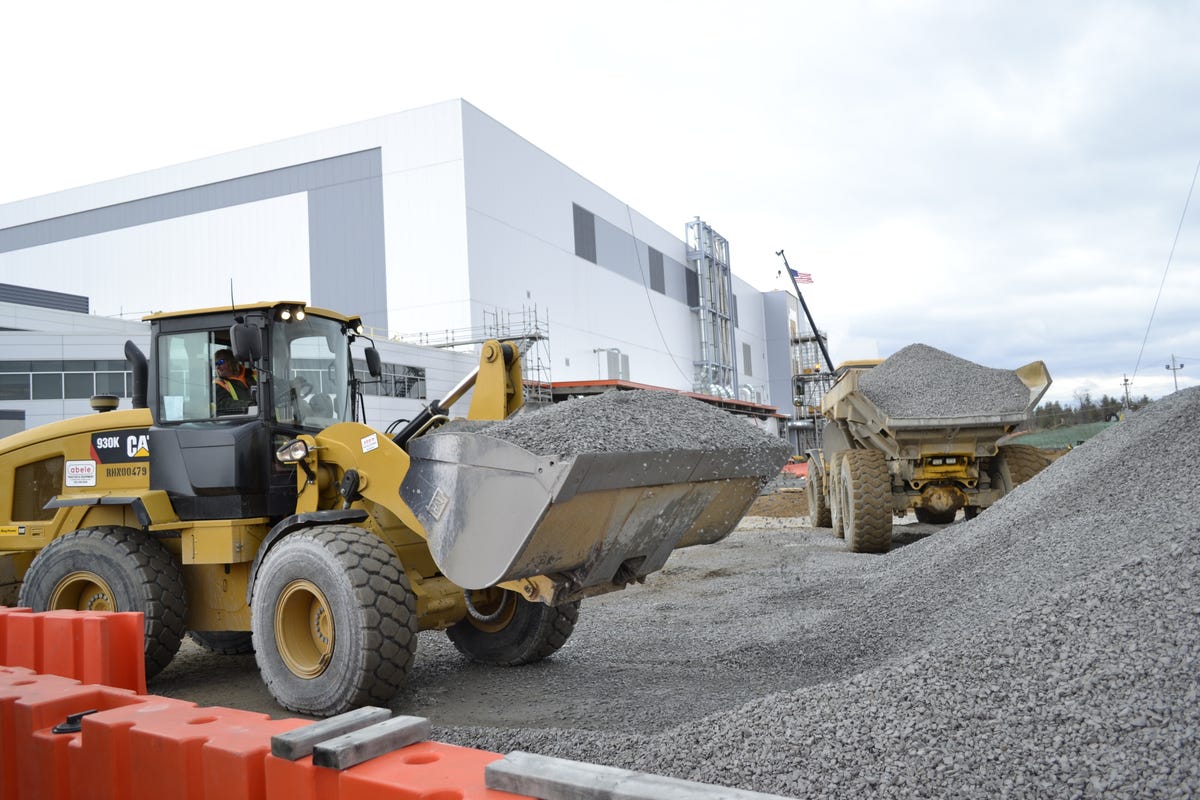
A few days before arriving in Oregon, I visited the rural town of Malta, N.Y., just north of Albany, where GlobalFoundries is expanding its $10 billion chipmaking factory on a 222-acre parcel. The drive up the hill to reach the factory looks like the tree-lined entryway to a state park. At the end of the road, though, a long, squat gray building fills the horizon, replacing the acres of trees that once stood there.


Ben Fox Rubin/CNET
GlobalFoundries, the former chip-production business of struggling semiconductor company AMD, is now privately owned by the well-heeled Mubadala Development Co. Mubadala was created in 2002 as the investment arm for the government of Abu Dhabi, and it’s poured billions of dollars into finishing the Malta facility so GlobalFoundries can stay competitive in the fast-paced market for chips.
I was allowed to walk through a clean room — a strictly controlled manufacturing space where chips are made — in Malta to get a closer look at the process of making such tiny transistors. (Both Intel and GlobalFoundries barred me from taking any pictures or video of their production floors.)
The clean room floor is windowless, with automated machines spitting out chips hour after hour throughout the day. The factory runs 365 days of the year. It’s easy to lose any sense of time inside this enormous room. The white-walled manufacturing space — stretching across 300,000 square feet — is bathed in yellow fluorescent light, which protects a lithography chemical called photoresist that’s used in the machines. Air purity is tightly controlled, with ducts on the ceiling blasting air-borne particles down at perforated tiles on the floor, then the air is scrubbed and recirculated.
There’s constant noise. The high-pitched hum of the machines stenciling, drawing and cleaning mixes with the whir of overhead hoist transports, or OHTs. An army of those upside-down U-shaped robots shuttle rounded containers stacked with chip wafers — autonomously racing across tracks on the ceiling and parachuting down to pick up and drop off their cargo.
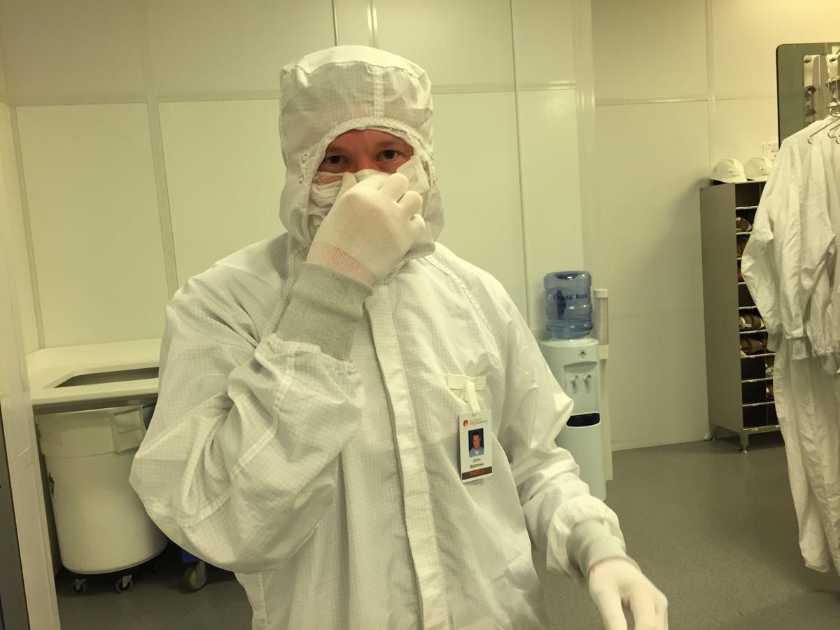
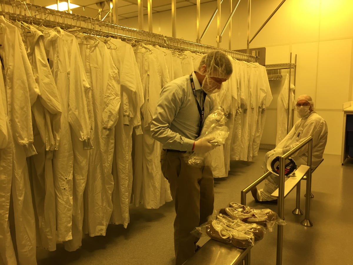
To keep dust and other particles out of the air, GlobalFoundries clean-room workers can wear only odorless deodorant. Makeup and perfumes are prohibited, and workers need to wait two hours after smoking before they can re-enter the facility. There are protocol police who canvass the floors to ensure compliance. To get into the clean room, I walk on several sticky, blue pieces of paper that remove the dirt from the bottom of my shoes. I then put on two pairs of gloves, a beard mask, face mask, a hood, boots, glasses and a white suit over my clothes. They cover nearly every inch of my body.

Ben Fox Rubin/CNET
Inside, workers shuffle about in cloth masks and suits, lugging pallets of floor tiles, sitting on the ground to build things from glass or metal sheets, typing away at indecipherable computer screens, and walking around with cylindrical vacuum packs strapped to their backs.
My suit is uncomfortably hot and stuffy, but John Mathews, the lithography section manager who shows me around, says folks get used to them.
Mathews points down one row of lithography machines — giant white boxes with darkened windows on some sides to show the robotic hands or other tools inside. They are the most expensive machines in the factory. “You’re looking at $1 billion,” he said, smiling behind his glasses and face mask.
In the middle of Mathews’ tour, as he rattles off acronyms — OHT, AMHS, FOUP — I ask about one of the dozens of candy-red buttons painted with the white letters “EMO.”
“Yeah, don’t press that,” Mathews warns me. “Emergency manual override. Press that and a tool can be down for a day.”

Ben Fox Rubin/CNET
Zapping dead frogs and the early march toward the modern chip
The silicon revolution is rooted in more than 200 years of scientific work marrying chemistry and electricity. It goes back to Luigi Galvani making dead frogs’ legs twitch by connecting them to strips of differing metals and Alessandro Volta building the first battery from discs of copper, zinc and saltwater-soaked cardboard. Those early experiments eventually led to Bell Labs, where a combination of gold, germanium and wires created the transistor.
Moore, born in 1929 in California, started to discover this world at an early age. He grew up using a home laboratory in his parents’ backyard to develop chemicals for bombs and rockets, according to the book “Understanding Moore’s Law.”
After graduating from the California Institute of Technology with a doctorate in chemistry and physics and helping start Intel’s precursor, Fairchild Semiconductor, he wrote a short piece for Electronics Magazine in 1965 called “Cramming More Components onto Integrated Circuits,” in which he predicted that the number of components on a chip would double every year. He co-founded Intel in 1968 and revised his forecast in 1975 to say that doubling would occur every two years.
Visiting the places that make Moore’s Law happen (pictures)


The ever-shrinking transistors allowed chip companies to produce faster, more power-efficient chips at a cheaper cost per transistor. It was like finding a way to create thinner and thinner rows of corn on a field, letting a farmer make more of the product and even sell it for less but still make more money. Moore’s Law was progress without compromises.
That 1965 article wasn’t just prescient; it became the tune to which all of technology dances. If Moore’s Law ended in 1995, “we’d still be carrying Nokia candy phones,” Hutcheson said.
“I didn’t expect this binary order of magnitude increase, the thousandfold increase in complexity to be very accurate,” Moore, now 86 and living in Hawaii, said in an interview with Intel earlier this year. “I just thought it was a general trend we were going to have. But in fact, it was far more accurate than I could have anticipated.”
The process of getting to the next advancement is getting harder, even as the pace of Moore’s Law hasn’t abated.
Lather, rinse, repeat
Sitting in a conference room in Ronler Acres, Bohr told me the research there goes on every hour all year long, at the same rate as any chip manufacturing operation. “We realized that in order to keep on this pace, our development effort has to be very fast-paced,” he said.

Ben Fox Rubin/CNET
And so it’s not uncommon for a Ph.D. process-development engineer to get a call at 2 a.m. from the factory with a report that his experimental chip wafer just spit out of the machines “with funny green spots on them,” he says. A response is needed right then so the experiments can keep moving forward.
Intel employs about 1,000 Ph.D.s around Hillsboro, more than the engineering faculty of MIT, Berkeley and Stanford combined. These researchers investigate and experiment with a variety of ideas. They have to: fewer than one in five concepts ever makes it out of the sandbox.
Bohr helps move the most promising ideas forward through development, which eventually leads to a new manufacturing processes for making transistors even smaller. Once a smaller-transistor process is reached, there’s little time to uncork Champagne — the cycle of lather, rinse, repeat doesn’t wait for celebrations.
Among the innovations Bohr and others at Hillsboro can claim are the development of a technology called FinFET, in which a transistor, instead of being made flat on the surface of silicon, is raised up into a three-dimensional form. Now chipmakers can create the equivalent of tall buildings, instead of squat, single family homes, allowing them to pack even more transistors into tighter spaces.
Other efforts include adding new materials and processes to make sure transistors won’t leak out their electric currents, even as they become smaller and smaller.


Ben Fox Rubin/CNET
“It takes much longer because the complexity adds raw process time to what you’re doing and then you’re adding more variables by going to different materials and different features,” Tom Caulfield, general manager of GlobalFoundries’ Malta factory, tells me during my visit there. “So the pressure on keeping pace is exponential.”
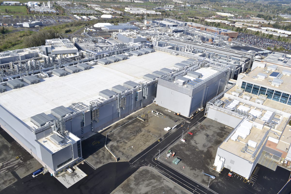
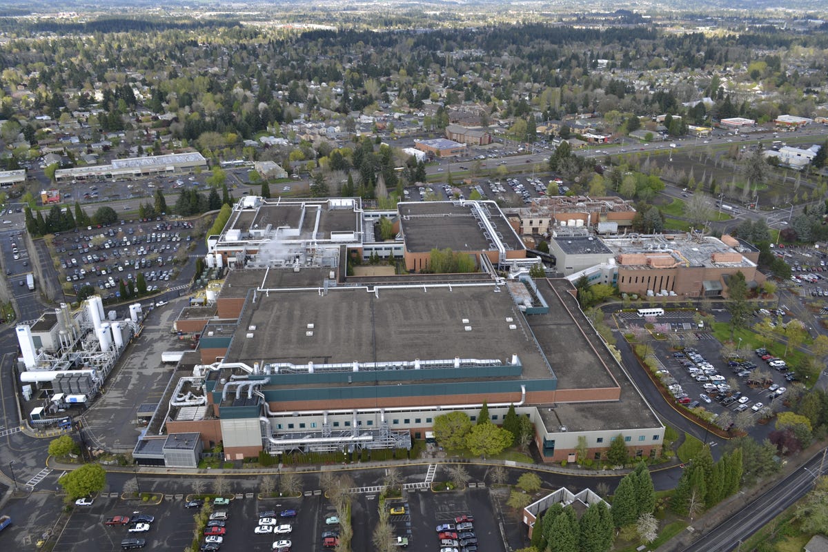
Ronler Acres is a testament to how elaborate Moore’s Law has become. Intel, based in Santa Clara, Calif., first came to the Hillsboro area in the 1970s, realizing all its existing factories at the time were along fault lines in California. It started with a handful of brick-facade factories, known as the Aloha campus. They now seem quaint compared to the hugeness of Ronler, where construction started in the 1990s.
In about two decades, Moore’s Law required bigger and bigger facilities. Work that could once be done in Aloha — roughly the size of a large suburban mall — moved to a mushrooming campus at Ronler, a mass of rectangular white-and gray buildings. They’re connected by a maze of stainless steel pipes and lattices, dotted with tall silos filled with gases and surrounded by a utilities building, water purification plants and an electrical substation.

Ben Fox Rubin/CNET
Intel’s campus dominates a patch of the quiet suburban town, and is surrounded by farmland and hills lined with Douglas firs, cedars, sequoias and spruces.
“The price will continue to skyrocket,” Sam Wang, a longtime chips manufacturing analyst for research firm Gartner, said about the cost of making chips. “The price has gone up so quickly, not that many companies can afford that.”


Ben Fox Rubin/CNET
Despite the challenges, Bohr, a 37-year Intel veteran who holds more than 70 patents, keeps working, driven by an urge to build new things. In high school, he made a reflecting telescope, grinding a mirror into a precise paraboloid so he could view the stars through the murky Chicago sky. Now his cubicle is filled with the things he’s helped make: walls are decorated with frames holding old wafers from the 1980s he worked on and a close-up picture of a cross-section of a computer chip from 1990.
It’s people like Bohr who show that Moore’s Law isn’t a law. It’s a force of will, perhaps an addiction, driven by a capitalist intent that has flooded the world with electronics and connected billions of people. What chasing Moore’s Law will look like decades from now is for future researchers to discover.
“I view myself and our group as pioneers,” Bohr said. “We’re off in the unknown, the uncharted territory.”


